Project Zero : The MCU (Programmer)
To begin the design and creation of the project I worked on the base board of the design.. The Microcontroller, an Atmega 2560 was chosen to form the programmer and interface to the whole system primarily because of its large pin count and also I happened to have a few left over from a previous project.
The Atmega is configured to run from its internal 8Mhz oscillator and to also output this out the CLKOUT pin so that later on this can be used to provide the system clock to the Z80, this is switched with a GPIO that can be used for single stepping support via a 74AC157 Logic gate. Almost all of the connections on the Atmega are used for the CPU bus and associated lines, this ties up 34 pins of GPIO on the Atmega. The Address bus and data bus are arranged such that they fall neatly on the ports of the atmega so that we can directly write bytes to the ports directly without any bit fiddling.
Schematic and PCB Design
As this is proabably the most dense board in terms of design, this board decided the layout of the headers that will rise up through the stack of boads for future.
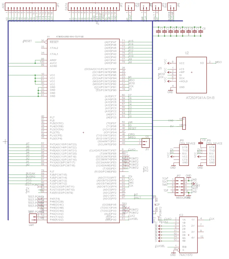
Messy and Complex, with one glaring mistake as well.. Oops
The giant block in the center is the Atmega itself, with the blue bus bar hiding all the ugly wiring that would be needed to breakout the pins to the headers at the top of the picture. In the bottom right we have the 74 157 that is being used to select between the two clock signal sources. Above we have two FTDI breakouts, one that is used for programming and one that is just for future expansion :) There is also a footprint for a usb micro that only provides power for running the unit on.
And now for my mistake.. the SPI Flash chip (the block in the upper right), when I placed this on the board I completely forgot that its a 3.3V only device. For now I have not populated this and will need to figure out how to modify the board to fit a 3.3V regulator at the minimum (and some protection for the IO lines as well probably).
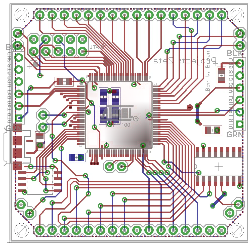
Fairly explanitory, complete with mistake SPI flash in the lower left
The PCB design is fairly self explanitory, with all the required wires broken out, also broken out is the JTAG connector that will be used to load the bootloader onto the Atmega and to allow for debugging in the future if required (hopefully not!).
Otherwise, i tried to breakout all the unused signals that i could to small connection test points that I can potentially use for future modifications to be made to this board.
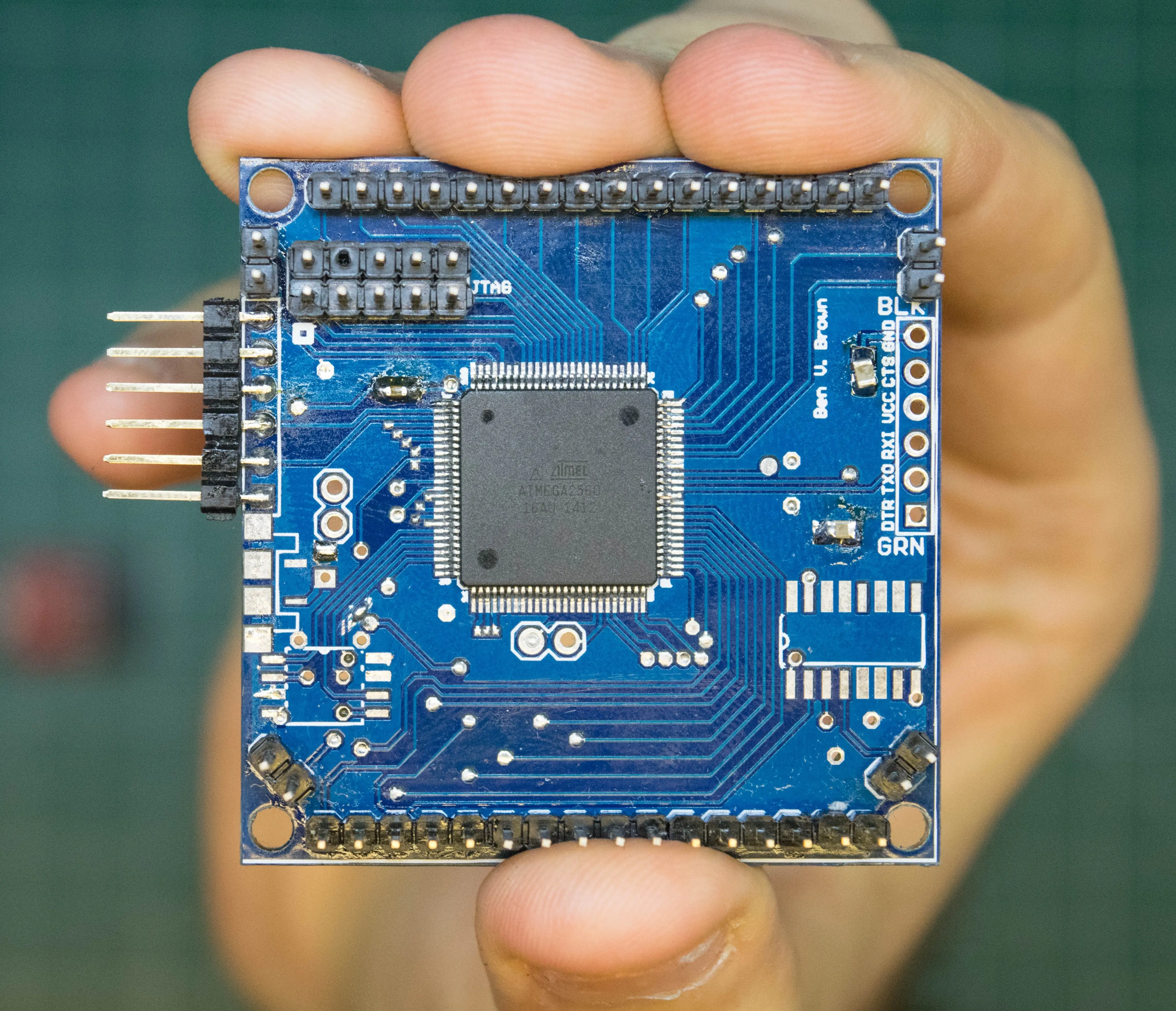
The final board, complete with the mess that flux loves to leave on everything.. Dont panic, it will be cleaned eventually.
Code
The board is running the Arduino bootloader to allow for quickly coding a set of libraries to get the board up and running.. Eventually I plan to migrate away from this, but for now it provides a nice environment to quickly get up and running. Note that the board is running on the internal 8Mhz RC oscillator, and thus the arduino configuration needs to be modified to account for this.
As always, all the code and design files for this project are available over at GitHub.