Project Zero : The RAM
In continuation of the development of Project Zeta, the small compact Z80 based microcomputer that I am slowly learning on, comes the next installment.. The RAM board!
Now this is actually performing double duty as the ROM as well, as the inital plan is to program the RAM at boot with the program that the system is to be executed.
Design
The RAM board is designed to provide a nice simple breakout for two 32k SRAM IC’s onto the memory bus for the Z80, nothing fancy here, no bank switching or real logic. We utilize two logic gates (7432 OR gates) to decode the output gating and the write enable on the two chips. Along with an inverter on the A16 line of a single transistor.

Very minimal design, nice and simple
The main two IC’s clearly visible in the center are the two SMD 32k SRAM’s The two I plan on using for this build were scavanged from old PCI cards and appeared to surive the hot air rework well enough to be worth testing. Below these there is the lone transistor that inverts the A15 line for the second SRAM (each being 32k each means that the highest bit of the address bus effectively becomes the chip select for each ic.). In the lower right are the two OR gates used to decode the read and write lines along with the MREQ line, this is used so that only memory access goes to the SRAMs (instead of the IO Request). You could technically design without this, but I liked the idea of being able to have the external IO line used properly so that I can extend the system later on for more IO peripherals.
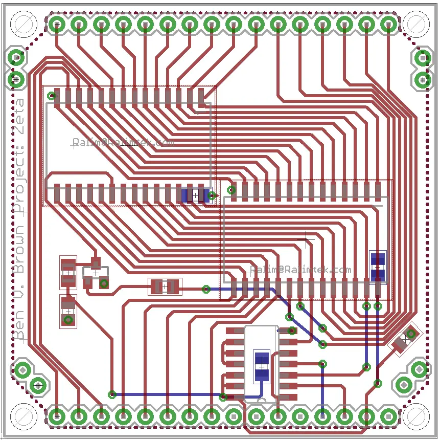
I love the look of the 45 degree sweeping traces..
The PCB layout was performed in Eagle cad, it is largely fairly simple with mostly just bunches of tracks trying to fit everywhere. Note the offset nature of the two SRAMs, this enabled me to (just) have enough room to route the lower set of traces with minimal Vias to the other side. Nothing overly complex really, small decoupling cap on the back of each IC. Originally I designed a dual footprint for the weird J lead variations of these as well, since I have a few hanging around, however the footprint of those is just too tight to let me get away with routing all the inner traces nicely.. If i really need them later on ill bodge them onto this footprint.
Physical
After sending the board design off to Dirty PCBs who did an amazing job of the circuit boards, I populated the two SRAMs and the OR gate.
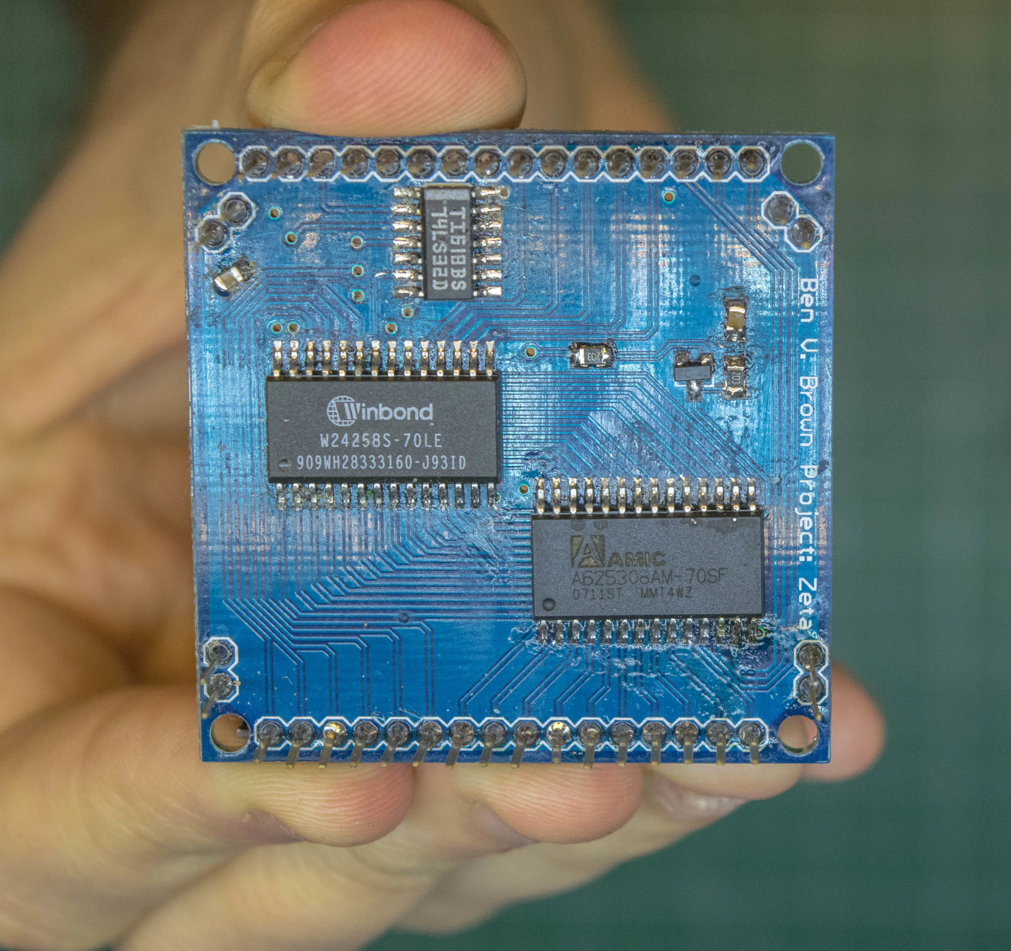
Here it is, the nice simple compact 64k of SRAM.. Just what the doctor ordered. Nice and pretty in blue as well!... Please ignore the gross mess of flux on the board for now, I'm all out of cleaner currently
After the inital population of parts, the board was connected to my bench supply and the current limit slowly raised, the board did not immediately catch fire which was a nice bonus.
Programming
To communicate to the RAM board, it was stacked on top of the Microcontroller board that sits at the bottom of the stack. The library for this unit was created with functions to allow reading and writing to the SRAM as well as a small memory test was written for the unit to perform on first power up.
Data writing to the SRAMs
To write data to the SRAMs the nice wrapper function writeMemory is used, this takes in an address along with a value. This then works to call further functions to write the data lines to the given states and latch this value into the SRAMs.
Reading
Similar to writing, reading works by driving the address bus to the wanted adress and then reading off the value from the data pins.
Memory test
This all forms into the first real work the system has undertaken, performing a RAM test on the boot of the processor.
The appropriate code:
bool memoryTest()
{
  byte testBuffer[] = {0x00, 0xAA, 0x55, 0xFF}; //values used for testing the ram

  for (uint32_t address = 0; address <= 0xFFFF; address++)
  {
    //loop through all index's and write the data
    dataBus.writeMemory(address, testBuffer[address % 4]);
  }
  for (uint32_t address = 0; address <= 0xFFFF; address++)
  {
    //loop through all index's and write the data
    if (testBuffer[address % 4] != dataBus.readMemory(address))
    {
      Serial.print("Memory Fail : "); Serial.println(address);
      Serial.print(testBuffer[address % 4], HEX); Serial.print(" : "); Serial.println( dataBus.readMemory(address), HEX);
      delay(10);
      return false;
    }
    if (address % 4096 == 0)
    {
      Serial.print((address >> 12), DEC); Serial.println(F(" OK."));
    }
  }
}
This code writes the given 4 byte pattern over the entire SRAM and then read back the values to ensure a match. This is not a overly complex or in depth memory test, but it works to check the physical connections (well and test my code as well).
As always, all the code and design files for this project are available over at GitHub.