In the new release of firmware for the TS100, I have moved the system from using a software-driven bit-bang of the output to hardware-based timers. The issue here is that we cannot just use normal PWM!
Why can’t we just use normal PWM?
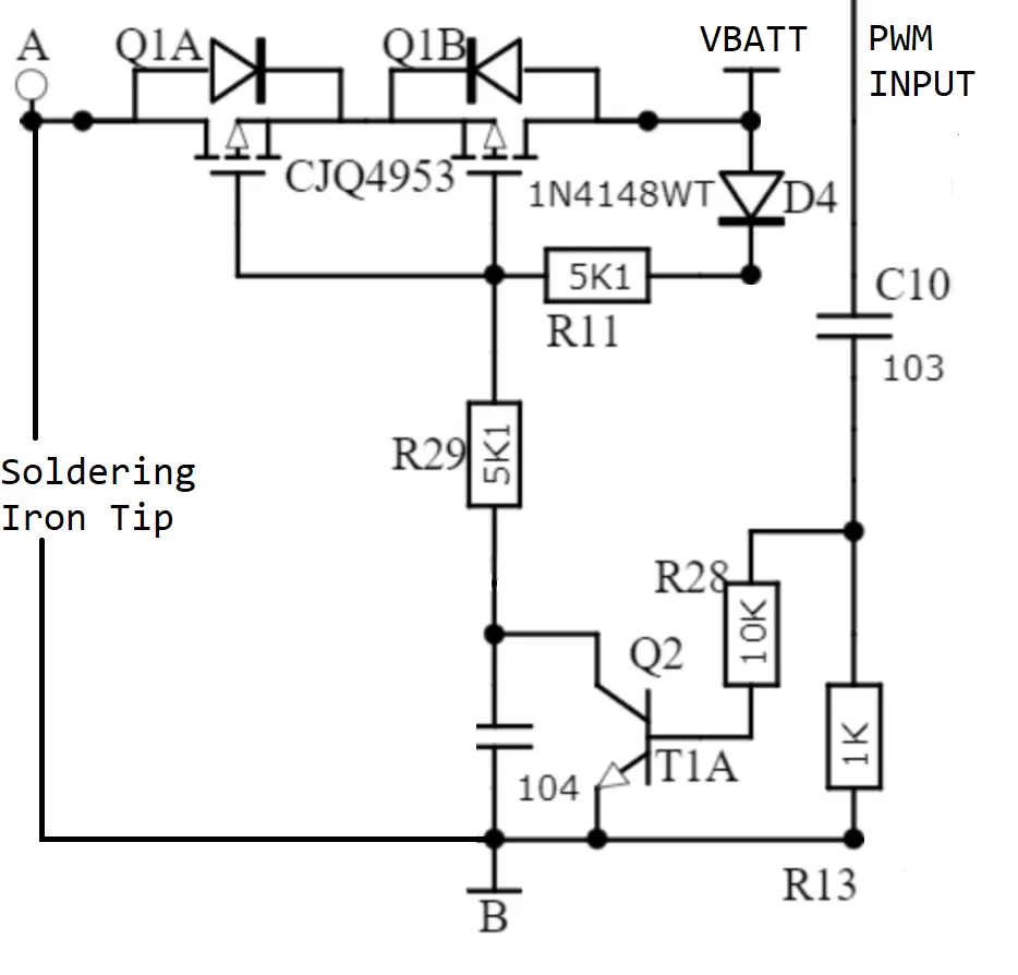
Soldering Iron drive Schematic
The above image shows a small extract from the TS100 schematics, with the PWM signal from the STM32. The soldering iron tip is driven by the back to back MOSFETs(Q1A/B). These are P channel MOSFETs, so they are on when the gate is pulled low relative to the battery input. R11 acts as a pullup to ensure the gate is high whenever it is not being actively pulled down via Q2 and R29. When Q2 is turned on it will pull the gate to half of VBatt (R11/R29 form voltage divider). The filter capacitor in parallel to Q2 acts to provide a turn-off delay on the gate so that the gate will stay low for a period of time after Q2 turns off. (Time constant is approximately 1 millisecond).
So in order to turn on the soldering iron tip, the transistor Q2 needs to be turned on and held on while the tip should be on. The problem arises as the base for Q2 is AC coupled through C10. This prevents normal PWM mode being used on the STM32 however it does also mean that if the drive pin is inadvertently left high the tip won’t heat (because the capacitor won’t pass the DC level).
In order to turn on the base of the transistor, we need to provide an AC signal (such as a high-frequency square wave) that can pass charge through C10 and turn on the base of the transistor. This means that whenever we have a rising edge on our STM32 output pin, the capacitor will conduct and pass that positive charge through to the base of Q2 and turn on the transistor. On the falling edge, we will then discharge the base of the transistor and pull it slightly negative because some of the charge will have been discharged through the transistor base and also through R13. R13 is required to ensure the base of the transistor is held at GND (off) while there is no signal.
This means that for each period of the square wave, Q2 will only be on for a smaller subset of the period, which sounds like we cannot drive this tip quickly, however the capacitor that filters the output of Q2 is here to help with that, as we can discharge it nearly instantly when Q2 is on (Q2 shorts its terminals) and it will keep the gate for the drive fets low for a few milliseconds, keeping the tip on. During this time we have to finish our period of the PWM square wave and aim to turn Q2 back on before the gate has charged up very much.
This means that we want to have a high-speed square wave being sent from the MCU that can keep Q2 on as much of the time as possible. In this firmware, we end up driving the pin at around 2MHz which is very fast and probably not the best for EMC regulations, but measuring the gate on the MOSFET it results in the gate being pulled down to half VBatt which is as low as possible because of the resistor divider.
Setting up two level PWM
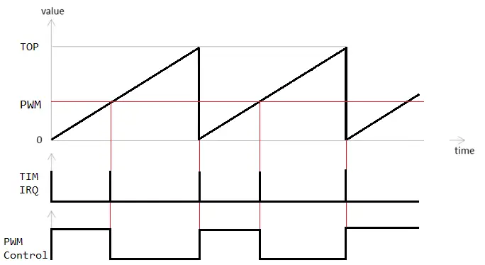
Using CCU IRQ to make PWM controller
As worked through above, we require a ~2MHz square wave to be created from the STM32 for ideal turn-on of the drive MOSFETs. Naturally the timer peripheral in the STM32 is perfect for this, however, this only gives us on/off control of the drive signal (enable or disable the timer). Which would work okay, but is not ideal, as it is nice to be able to have PWM control of the output to give extra control over the drive signal.
To solve this we are setting up two levels for the PWM control, where one-timer provides the 2MHz square wave that is used to drive the irons drive signal, and this timer is then modulated by another timer to provide PWM capability in the drive signal. This, unfortunately, has to be done using interrupts as you cant chain the timers in this way (that I have managed to get working so far). This does mean there will be 2 interrupts occurring for every PWM period.
This can be accomplished using one of the Capture Compare Units in the timer to create an interrupt at a set level of the timer. When this interrupt fires, we can disable the timer that is making the 2MHz drive signal. Combined with the timers interrupt on overflow, we can construct a PWM controller, where we use the overflow interrupt to enable the output and then when the CCU interrupt to disable the output.
This is shown in the above timing diagram, with the vertical red lines showing the interrupts that occur. The 2MHz square wave PWM output is controled via the interrupts so that its enabled when the shown output above is high.
Temperature measurement
The soldering iron brings in another complexity to this entire control system, where the temperature sensing works by having a thermocouple style join in the tip as part of the heater wiring. This saves wiring to the tip and is how the tip works with only two connections. However!, this has the problem that you cannot measure the tip temperature while driving the tip with power, as the thermocouple reading is tiny (microvolts per degree K).
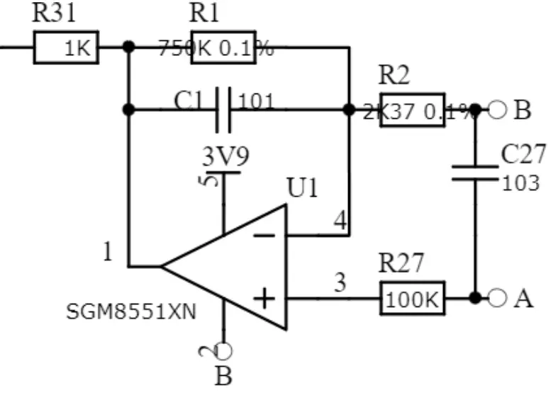
The A & B are the same as before - the iron tip connections
The TS100 has an op-amp setup to read the small voltage from the thermocouple (U1). This scales up the small measurements from the tip to the 3.3V range of the onboard ADC of the STM32. Note that node B is grounded, so the signal is present on node A. The 100K resistor is important as well as there can be up to 25V when the tip is being actively driven.
This op-amp directly feeds an ADC channel on the STM32.
Scheduling ADC measurements
We need to measure the tip temperature when the drive power is off, however, we want to perform this as soon as we can after the tip going off as this reduces wasted time when we could be putting this into heating the tip instead. As we are doing the two-level PWM, there is nothing stopping us from having the PWM timer go higher than the maximum that we allow the CCU (PWM channel) to go to.
For example, if we set PWM to only go 0-100, we could have the counter count to 150. This would give us 50 ’ticks’ of this timer where the output driver is guaranteed to be off. Taking this a step further, we can set up another CCU to trigger an interrupt when the timer reaches a value such as 125, that we could then use to start an ADC measurement while the tip is off.
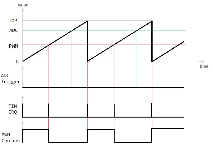
Using CCU IRQ to make PWM controller & start ADC
Shown above is this concept, where we have an extra comparator that is set up to trigger somewhere between the maximum PWM and the end of the timing cycle.
Injected ADC
This would be great if we had an ADC we can just set up to be ready to go and sample the input as soon as this interrupt arrives, but the ADC in the chip is already busy measuring the battery voltage and ambient temperature with DMA setup. Because this is set up with DMA we cant just randomly change its input channel as its unpredictable where DMA would shuffle that response into the output buffer, which means it would randomly overwrite the normal measurements.
The designers of the STM32 were smart and knew that this situation is actually really common in some control systems, where you want to be able to make the ADC sample a different channel immediately (drop what you doing and start this now style), but also not have it mess with DMA.
The injected mode is an extra option you can setup for the ADC in the STM32, this mode is designed to inject a request to sample channels when it is trigged. So this lets you set up ahead of time the channels and their settings. Then when the trigger event occurs (hardware or software) the ADC will the abort its current conversion and start on the injected channels. The results of these conversions are stored in their own registers that can be read by software. This means that the results will not interfere with or trigger the ADC’s DMA preventing issues of corruption of the data.
This injected mode works perfectly in this case, as we can have it be triggered with the timer CCU in hardware. The ADC has hardware trigger support for some of the CCU’s on the timers so that you can set up this system, so by selecting the timer, we use for the software PWM carefully we can utilize this hardware connection and prevent another IRQ occurring during the cycle.
Because the results do not interfere with the DMA, we do not need to change any settings or details with the DMA engine itself, as it just will not receive the interrupt to read the data register until the ADC completes the next sample after the injected channels are done.
We can configure up to 4 injected channel measurements that are completely isolated, so for the TS100 they are set up to all sample the tip temperature as this is the only measurement that we need to schedule to occur during the dead time of the tip drive signal
Overall solution
There are small implementation details that make this system less than ideal, such as the slow turn-off period for the tip drive MOSFETs due to the filter capacitor which means that there must be padding added between the PWM turning off and taking the samples on the ADC. This is why in the TS100 code, PWM is 0-100, and then the ADC is triggered later around 120 and then the timer counts up to 140. The injected readings are read by the PID thread whenever they are needed for use in the algorithm.
So, in summary:
The system has one main timer that has two Capture Compare Units (CCU) that are used to coordinate the software-driven PWM and also the ADC readings. This provides the benefit of the synchronization required when the ADC reads the tip temperature.