Where we left off
Part 1 covered the quick run down of selecting the STM32 and assigning a rough pinout in STMCube. Part 2 here will run through the schematic capture process and pcb layout at a high level.
Schematic Capture
I design exclusively in KiCad now, having completely moved off other platforms over the past few years. As such this guide will only cover KiCad related design work. I highly reccomend using hierarchical sheets in your design, to allow for both (some) reuse, as well as make the seperate building blocks clearly definied. Please, please, do not just throw your entire schematic on one page, it makes for a highly unreadable schematic for anyone else who comes along.
Approximate Schematic steps
- Create a new project in KiCad
- Make sure this project is in
gitor your selected version control software - Open up the main base schematic and place hierarchical sheets for each sub component
- Define hierarchical pins in each sub-sheet to be connected in the higher layers
- Add components to each sheet and connect to the hierarchical pins
- Sanity check STMCube against STM32 in schematic
- Start PCB layout
Adding Hierarchical Sheets
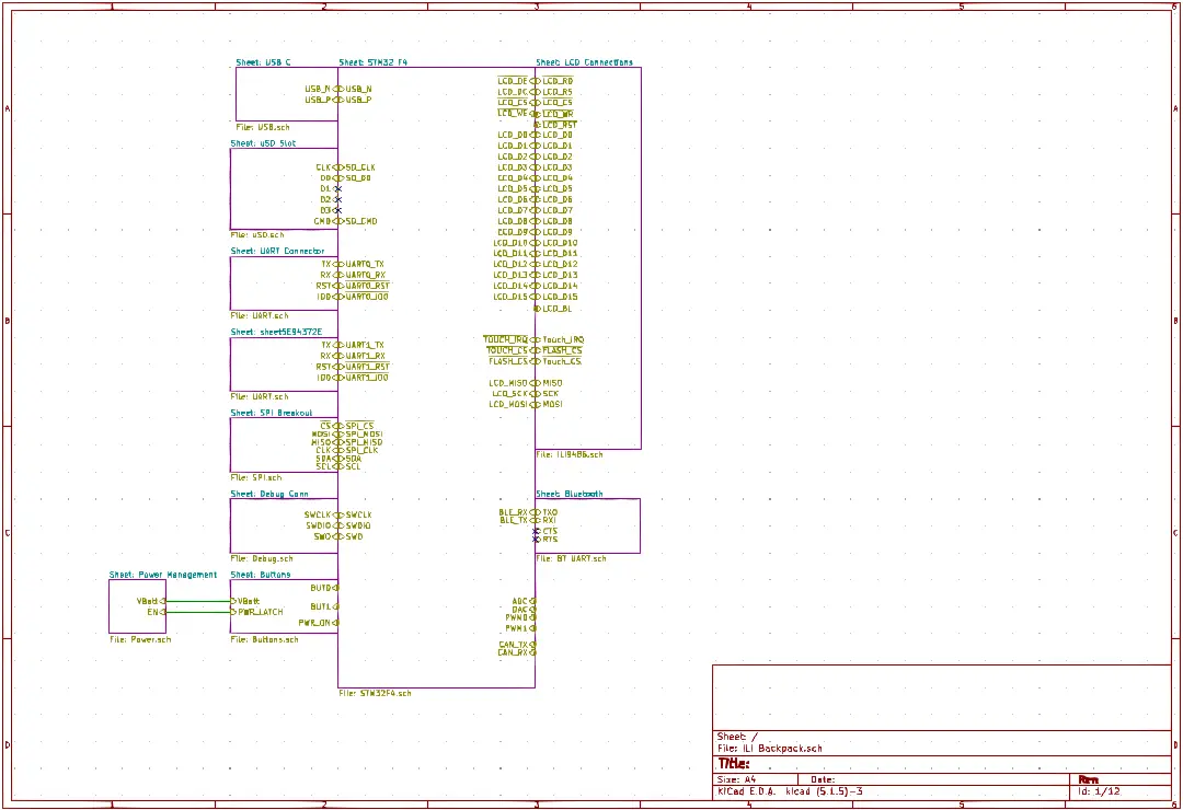
I highly reccomend creating blank sheets first, as these allow you to quickly work out your building blocks for the device. I place the STM32 in the middle and attach extra sheets around the edge to try and indicate how things interface. This works well enough for most things, with power being the main block that gets put in weird locations.
At this point, you mostly aiming for a high level outline, so for example, below is an image of this project with the pins defined as well. Notice how each sheet has a logical name that tells you what is inside that sheet. Dont try to be overly specific here as you want it to be readable at a glance. I reccomend setting the grid to 0.6mm, one step less granular than the default. This makes it easier to line up things easily by including one “snap point” between items. I also try and shape boxes to stick to the major lines to keep things roughly in a grid layout.
Also of note, is that you can select (drag over) and then duplicate sheets. This is handled in a manner of a second copy of the sheet that will link through to the first. If your design contains any amount of repetition I highly reccomend using this feature! This means that when you double click on one of these sheets to “go into it”, it will take you into the same file. This means changes and bug fixes automatically update the other references. This is really powerful when designing circuits with lots of duplication, as you avoid having to make the same change multiple times.
Rough Schematic
Checking the STM32 Pinout
When adding the STM32 to KiCad it is very daunting to have it spawn in with its 100+ pins that need to be connected. When I am at the stage of assigning the pinout to the STM32, I go to STMCube and un-pin every signal in the right click menu. Then as I add a singal to KiCad, I pin that signal in STMCube as well. This provides a quick indication that, that pin is “done”. Moving around the chip does require jumping around KiCad a bit as the pins are laid out in ther logical locations (not physical). However, this is usually not a big deal as you can quickly move to where it is once you remember the ports are in alphabetical order clockwise around the IC.
I also reccomend changing this sheet in the schematic to portrait mode. This does make it awkward when printing out, but it means there is plenty of whitespace around the IC for supporting circuitry and notes.
When laying out the schematic, I suggest thinking about if a signal needs to go to an upper level or not. For example, reset for the STM32 does not normally need to move up a layer as it only needs a pullup which is suitable to add to this sheet. I also reccomend adding pull-ups for I2C here as well, as if you have multiple devices on the bus, its not clear where these should be with the devices, but placing near the master (STM32) is logical enough most people will check here first.
PCB Layout
Laying out the PCB is the most time intensive part of the hardware design process. Attention to detail is critical and willingness to adjust as you go is really helpful. Expect to adjust your pinouts in STMCube and the schematic editor as you go, as pins may turn out to be in awkward places, and in this case moving a peripheral may be easier than moving to a 4 layer pcb design for example.
PCB Layout steps
- Assign footprints to all of your components
- Update PCB with F8
- Group all the parts into logical groups (all the battery management nearby for example)
- If board outline is known, draw it in
- Add any known mechanical mounting points
- Locate any fixed connection locations
- Lock in place points 5 and 6
- Roughly place parts in desired locations to minimise length of ratsnest lines
- Tidy groups of components to minimise the number of ratsnest lines crossing over (shuffle pins in Cube if you can)
- Finer pass checking all the components you expect are here and the design roughly fits
- Start laying out and wiring up components near fixed items (e.g. connectors)
- Move across the board from these laying out components where easy
- Once roughly routed, pass again to cleanup tracks
- Tune track lengths where required
- Clean up device labels
- Add Name, Date, and product name to PCB
- Sleep on it (and send to co-workers to check)
- Revise and order PCB
Many steps, but most are quite logical :)
PCB Steps screenshots
Start - Import all the footprints
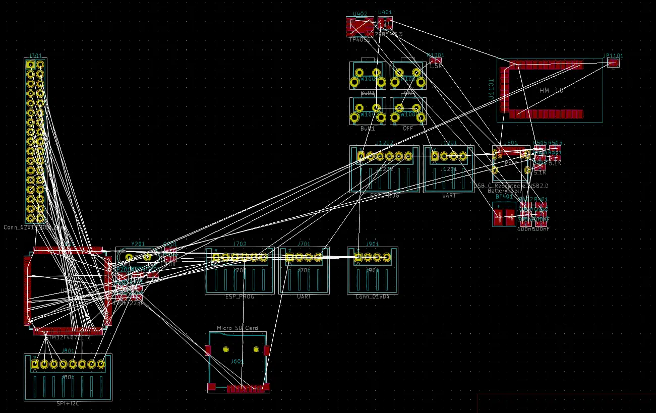
PCB 1
When first importing all of the footprints into KiCad it will tend to dump them all roughly grouped by their sheets (another reason to use these).
Locate Mechanical components

PCB Mech
Using the drawing files for the LCD modules, the outline is drawn in and the mounting holes and connector are placed.
After placing the footprints, edit them and set them to be locked so you cant accidentally move them later on.
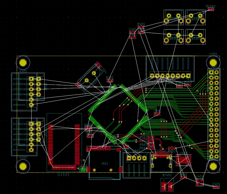
Rough place
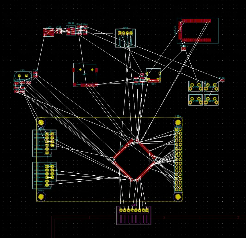
PCB Rough Placement
Roughly placing the components around into groups to minimsie the ratsnest. By placing the components into groupings helps clean up the design and location components into logical groups.
This also helps give a feel for size of the groups to start planning their rough placement
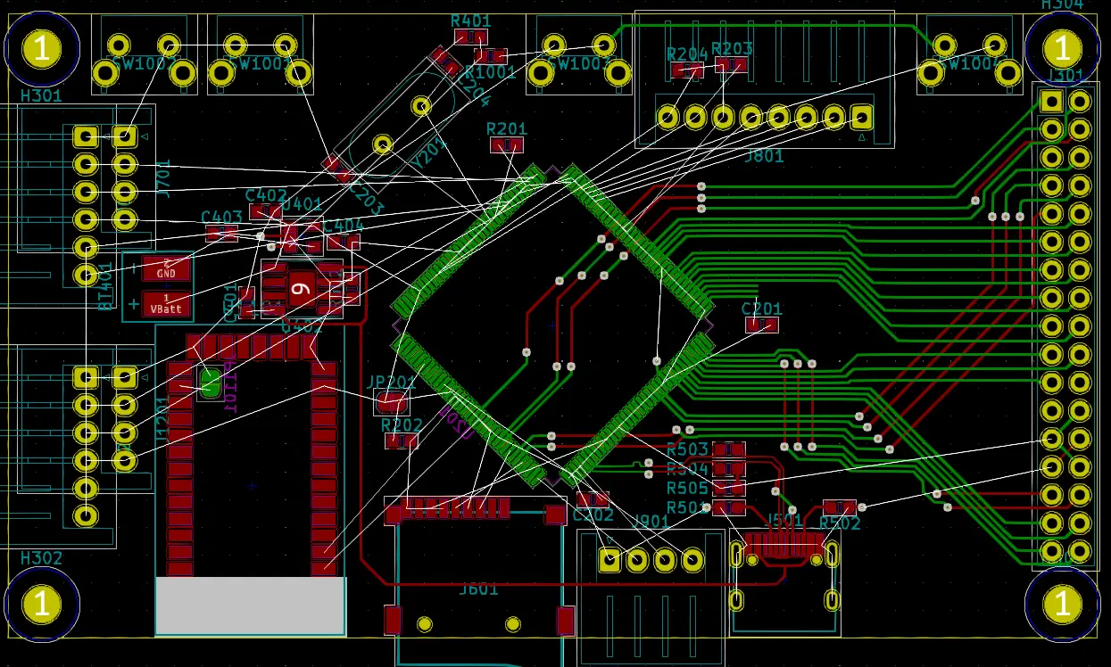
Flip!
PCB Rough Placement
In the previous photo, its quite obvious that the ratsnest is an absolute mess near the LCD interface on the right.
A good option to remember for sorting these out when you can’t reshuffle the pins, is to check if flipping one of the components to the other side will help with routing.
In this example, the LCD interface is almost perfectly backwards, so flipping the IC to the back of the PCB dramatically improves the ratsnest complexity.
You can also see how I often partially route the signals away from the TQFP to help improve readability of the ratsnest.
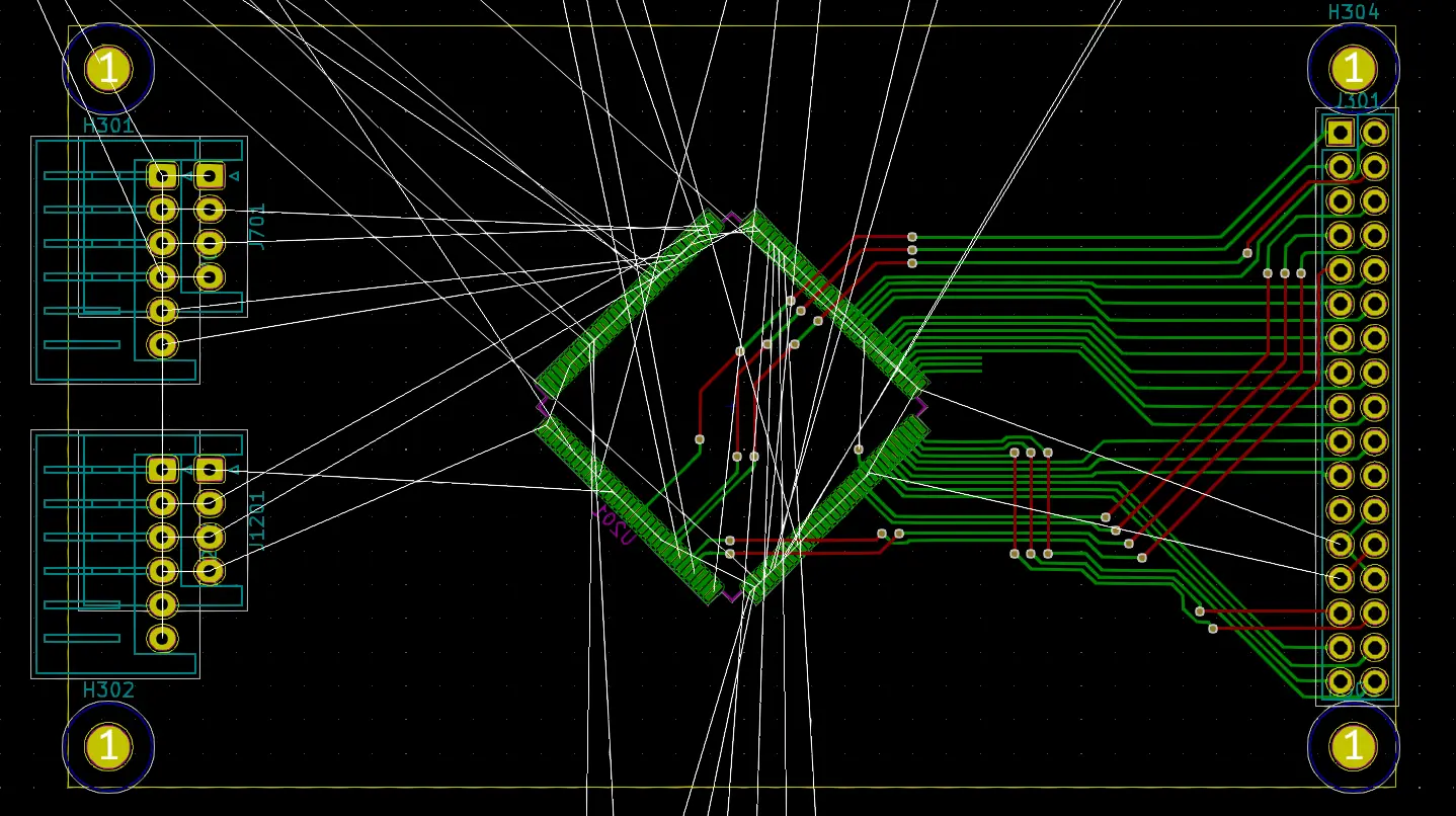
Shuffling Pins
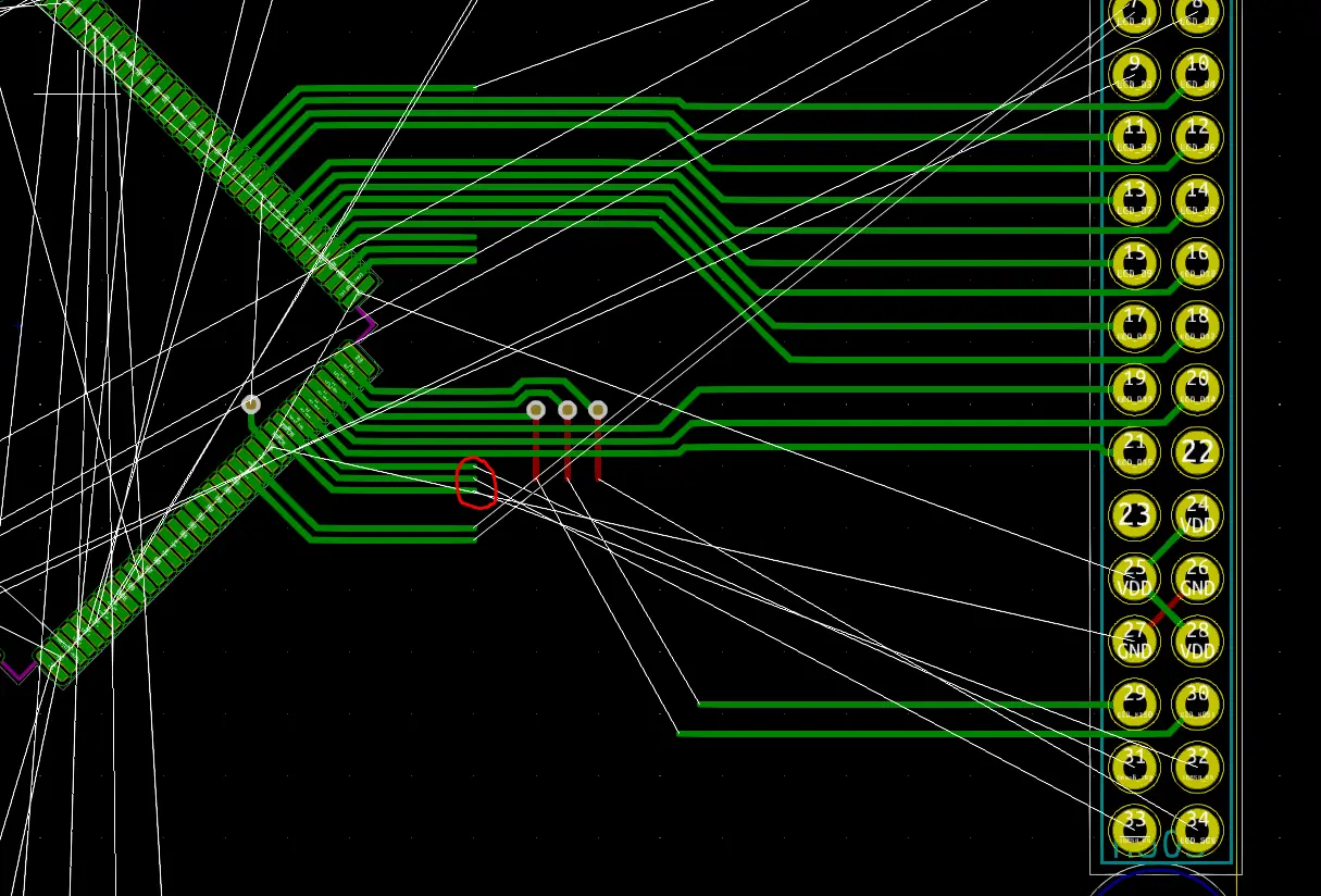
PCB Swapping Pins
This is a dedicated example of the mess that is easy to fix.
In this image, the circled traces are the movable pins for the LCD’s SPI port. These are the chip select and interrupt lines.
These are able to be re-assigned in Cube and the schematic to prevent this cross over occuring here.
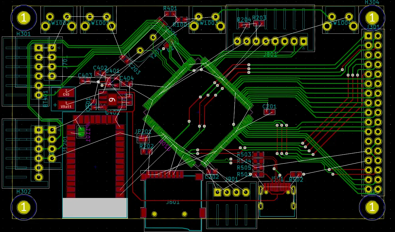
Test Fit
PCB LCD Routing
As the LCD interface is the most complex on this board, it is fully routed first to figure out the amount of space required for the traces.
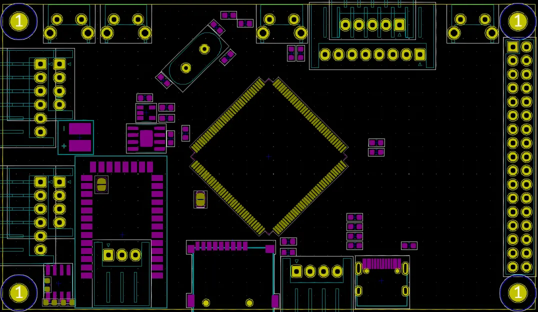
Packing
PCB Routing
PCB Routing
Now that the LCD interface is routed, all of the other groups are slowly packed into the board outline.
This board is going to be a tight fit on two layers, but should fit. As the LCD interface was the first routed, working outwards from its connections allows to pack closely without re-routing everything when one part does not fit.
PCB Routing
PCB Routing
PCB Routing
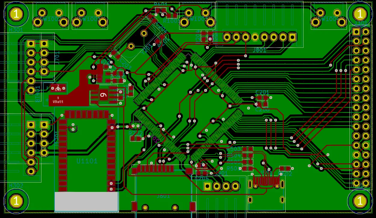
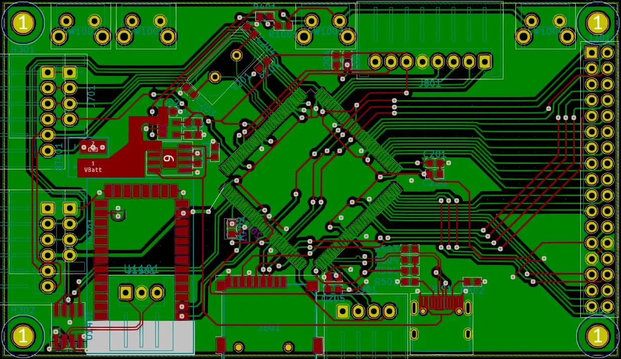
Final routing
PCB Routing
PCB Routing
PCB Routing
The final routing of the PCB, with the CAN chip an extra PWM pins crammed in.
Flood fills are used on the front of the PCB to space fill for ground and VDD.
NOTE: In this design the flood fills are different voltages, which means use of screws could short these because of lack of clearance. This was fixed later on after the screenshots were taken
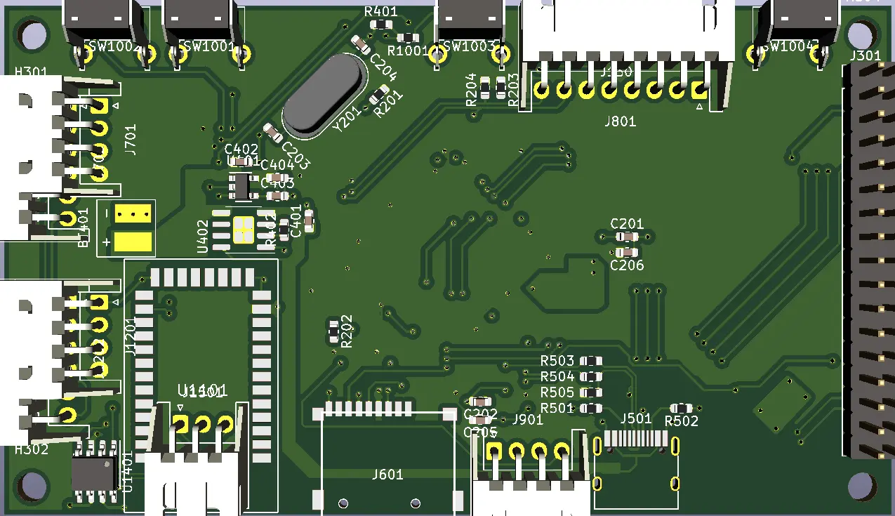
Remove and cleanup Silkscreen
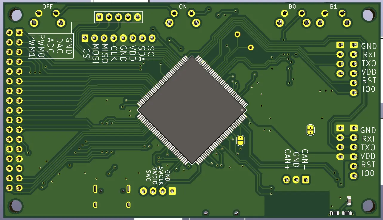
Removing Silkscreen
I personally prefer to not have part designators on the silkscreen on my personal boards. Mostly as it looks cleaner and most of my boards tend to not get cases or get clear cases. To do this easily, turn off the copper layers in the top right of KiCad.
This is a personal choice really though :)
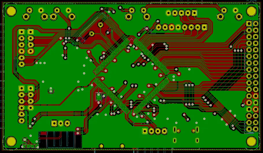
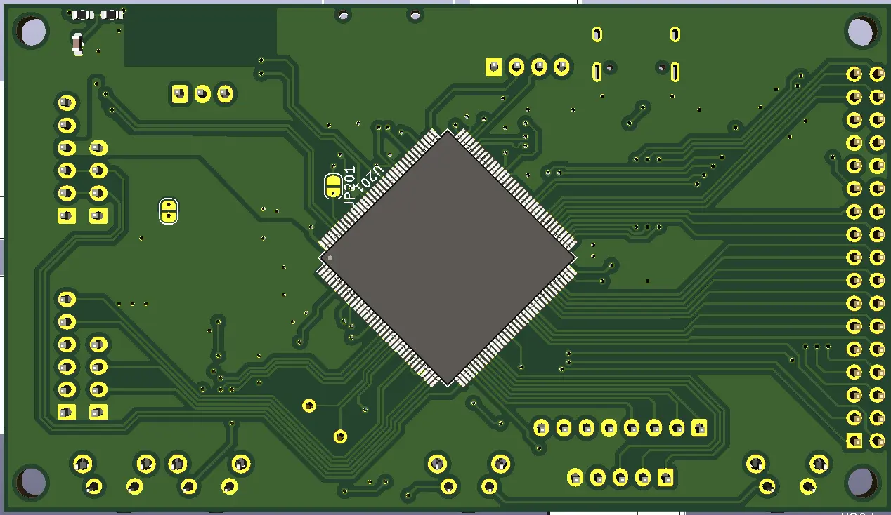
Final PCB
Final PCB Read
This is the view of the rear of the final pcb (the front hasnt changed). Notice the nice clear labels for all of the pinouts in the silkscreen.
Next Steps
After the PCB is finished, generate the gerber files and send these off to your selected PCB Fab. Also make sure to order components as well so that your not waiting for these when the PCB turns up.