Where we left off
Part 1 covered the quick rundown of selecting the STM32 and assigning a rough pinout in STMCube.
Part 2 provided a quick through the schematic capture process and PCB layout at a high level.
Part 3 covered exporting the PCB for manufacture and a quick run through the ordering process with PCBWay.
Disclaimer
In this section, I’m using PCBWay for the ordering process example. They have kindly offered to cover the cost of the production of these PCB’s before this series actually went live. They offered some free PCB’s around the time I was writing part two, making it very convenient to use their services for this series of posts.
Reviewing the PCB for quality
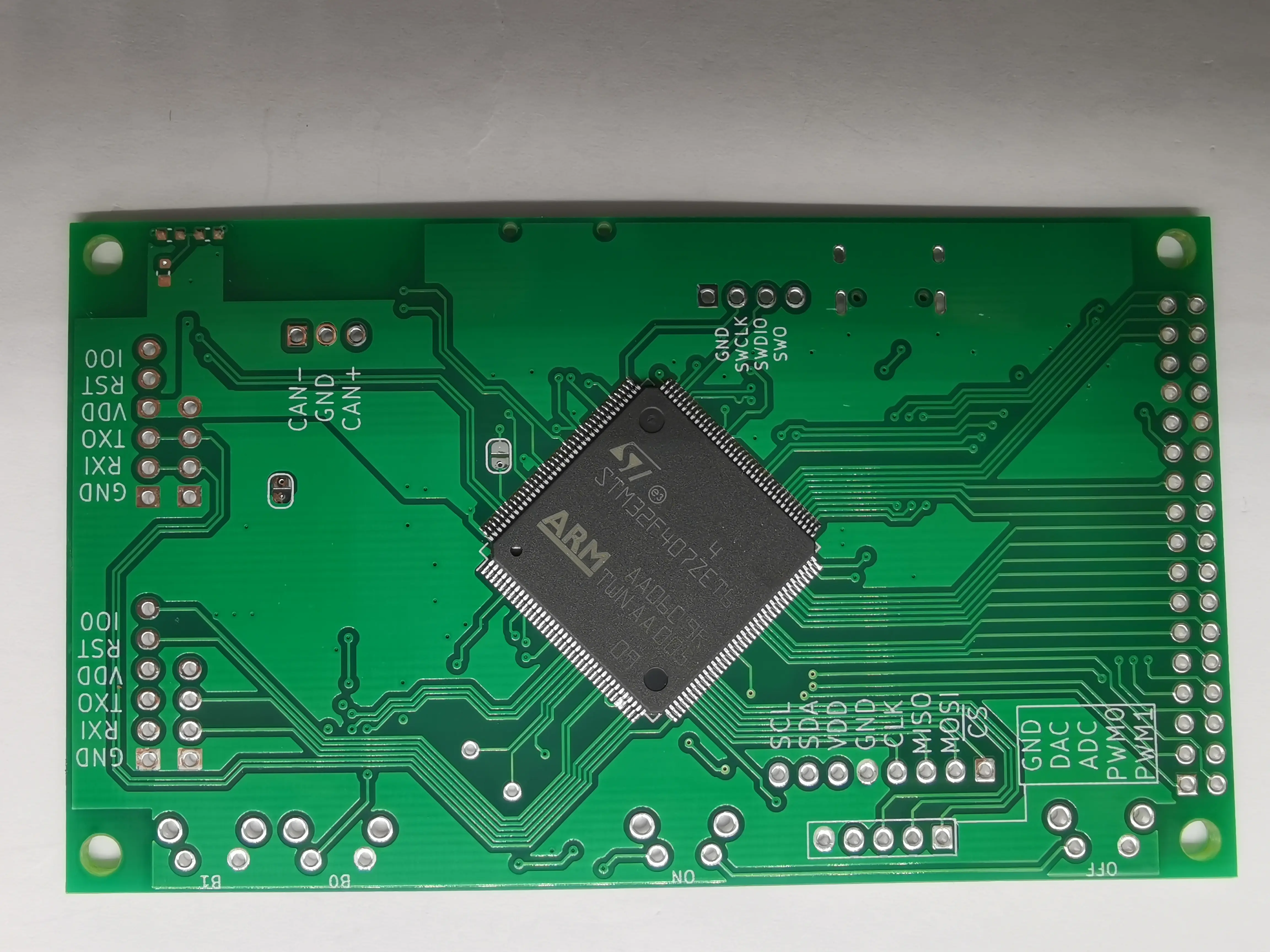
When the PCB’s first arrive back from the fab house, the first step is a quick visual check of the PCB against the 3D model.
Main points you are looking for here are:
- Is the PCB built correctly
- Are there any shorts (common near via’s for example)
- Are the drill holes through vias centred (easiest to check)
- Is the solder mask near the IC’s how you specified
- Is every trace you expect there
- Mechanical fit: Check the finest PCB footprint to make sure scale is correct
- Silkscreen and solder mask quality
PCBway checks
PCB is built correctly
The first check is to compare the PCB against your design files and sanity check that it looks as expected. At this point, you are not looking for exact dimensions, but more everything is where you expect it. If you notice anything that doesn’t match your designs, reach out the PCB fab group as fast as possible. You want to start conversations as soon as possible to make sure that there is no question around if it’s their order or not.
I’ve only had issues once that the PCB house didn’t catch (they have their own internal QC checks too). This was a case of a small pad being entirely missing from the PCB on some of the units. This was sort of a flawed design as the pad was very small and had little to hold it down to the PCB. In this particular case enough of the boards were correct that is not a show-stopping issue (always have spares).
Quality of the footprints
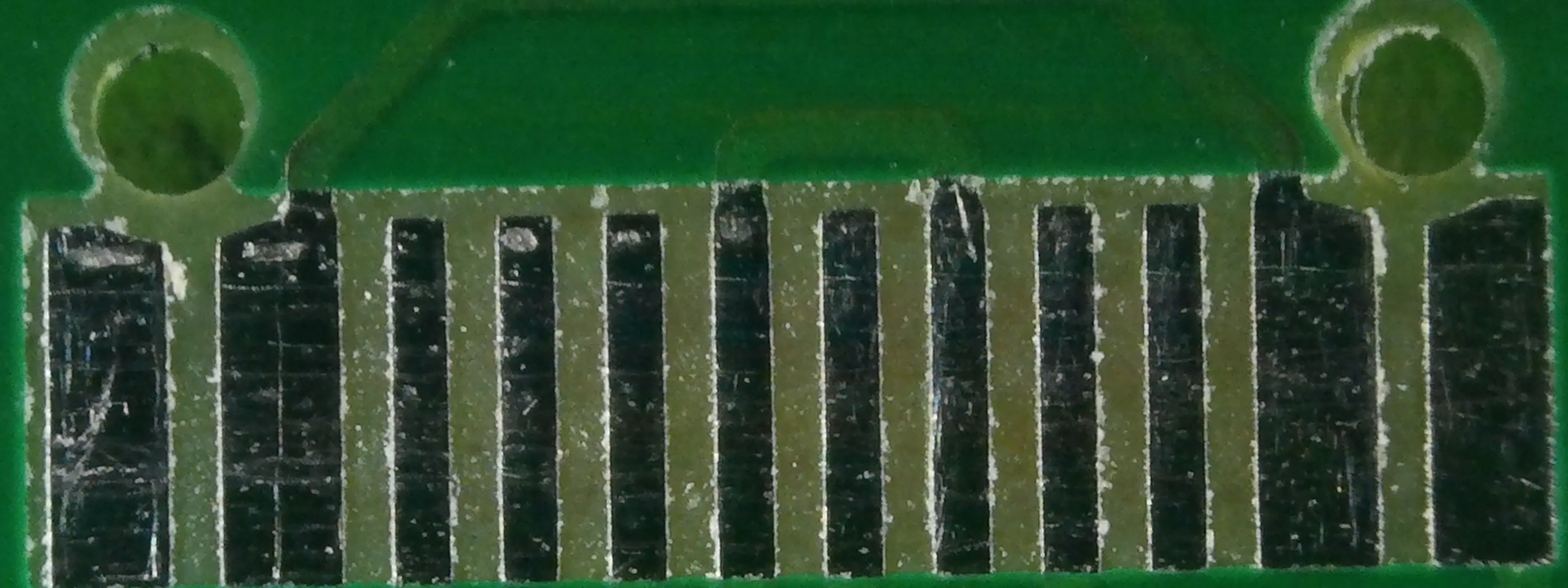
usbc
Looking at the USB-C footprint, all of the pads are etched correctly (no rounded corners). The solder mask is cleanly masked away from the footprint (nice rectangular cutout). The holes milled in the PCB are also in the correct locations, and no damage is visible.
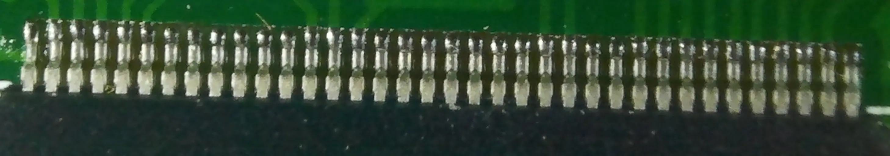
Quality of the vias
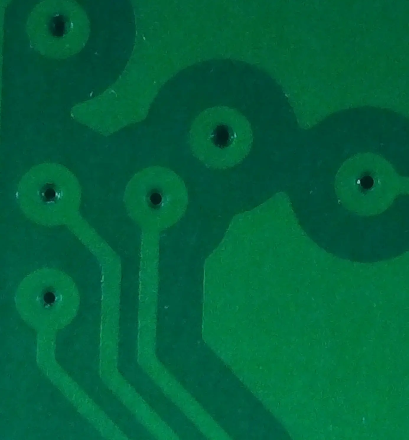
vias
While this design is not pushing any limits. It a very good indication of their quality control that all of the drill holes line up in the centre of the via pad (within reason).
Silkscreen & resist quality
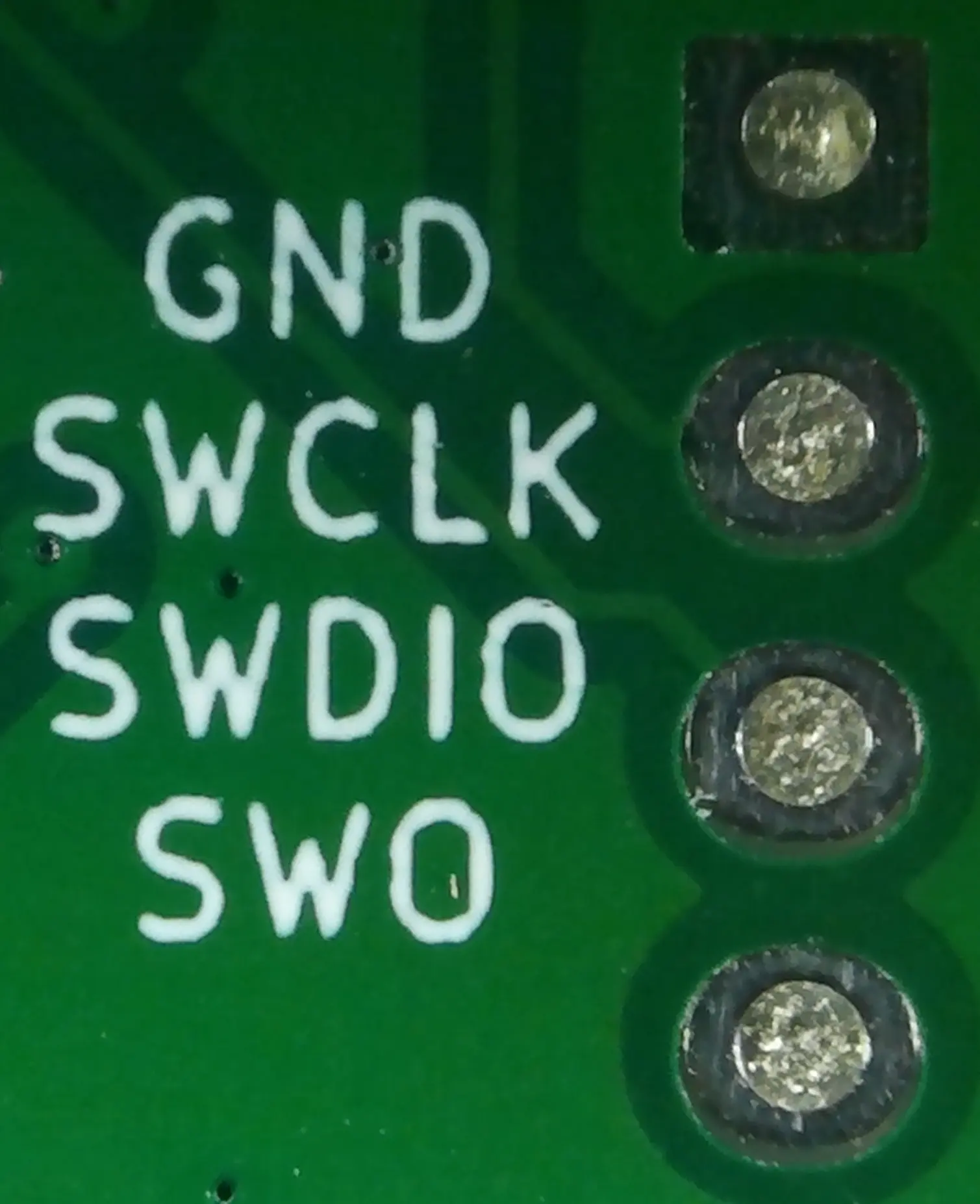
silkscreen
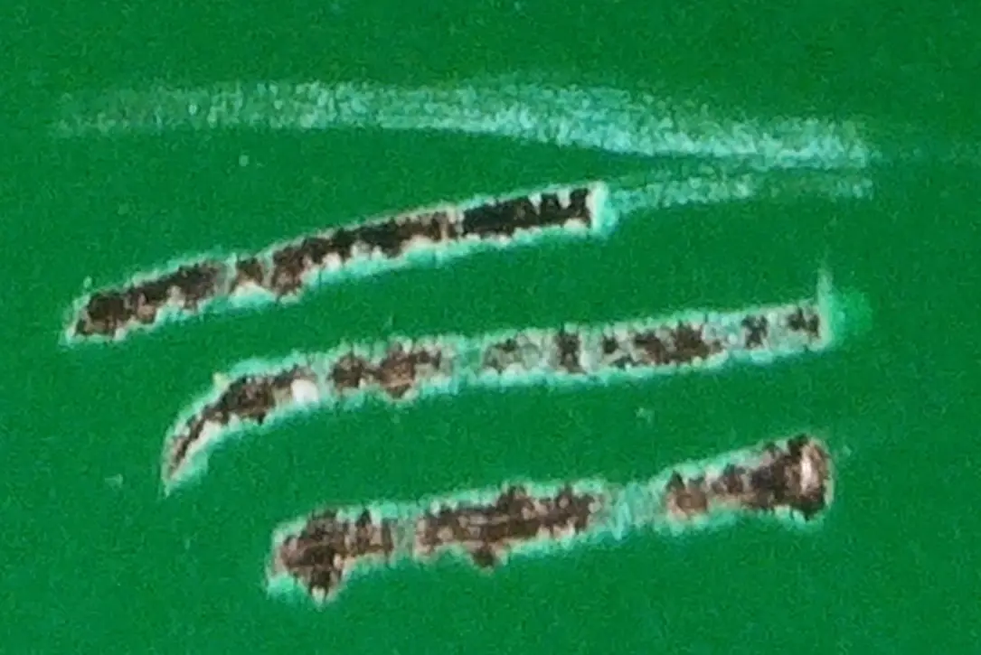
soldermask
Looking at the silkscreen print quality, you can see the slight unevenness in the printing that was used to apply this layer. However, it is massively better than the quality that dirtypcbs will usually turn around.
The second, random-looking scratch is created by dragging a sharp tool across the surface of the solder mask. Key features here are looking for the solder mask flaking off (which some JLC PCB’s have done). Soldermask quality
Extra steps for PCB Assembly
Good assembly groups will contact you with a photo of the first unit assembled to confirm it is correct. I highly recommend groups that reach out like this, as it prevents you from ending up with a set of PCBA’s with the TQFP on the wrong orientation. Yes, this has happened, and yes it will happen again.
Sample of contact image
PCBway check image
Above is the image that was sent to me by PCBway. The first thing is that is a very clear photo so that there is no doubt about the orientation of the components. In this order, I only had the assemble the STM32F407 as the TQFP is certified not fun to solder. The soldering job here is absolutely excellent (much better than what I can do). The image is their original file, no editing on my side.
The keen-eyed among us will notice the two pads that appear to be shorted, however referencing to the previous design, these pads are meant to be connected so there is no issue in the soldering here. Because of the way that the boards are constructed by default, there is no solder mask between the pins so the solder will flow across the linking copper and join the pins.
Check for shorts
shorts
Just because they did a very neat job on the soldering, it’s still work looking over every join carefully to double-check there are no small shorts hiding between the pins.
Assembly
If you need to assemble your PCB, there are a few key points to use when performing the assembly:
- Think about the order of assembly, if you have devices on both sides of the board, think about order. Also, think about clearance for a soldering iron if you are using one for assembly.
- Try and assemble one side first so it’s still easy to hold the PCB
- If you can, assemble the cheapest components first, and then test them before the remaining parts
- Test for shorts before you apply power
After the board has been assembled, test for shorts between the ground and any power rails. Also if you have more than one power rail check for shorts between these as well. Nothing is as much fun as desoldering dead parts because you run 5V on a 3V rail. Once all the power connections check out, power up the board on a current limited power supply to check for weak shorts.
If the board powers up as normal, move on to generating the base code from CubeMX and starting the firmware development cycle.